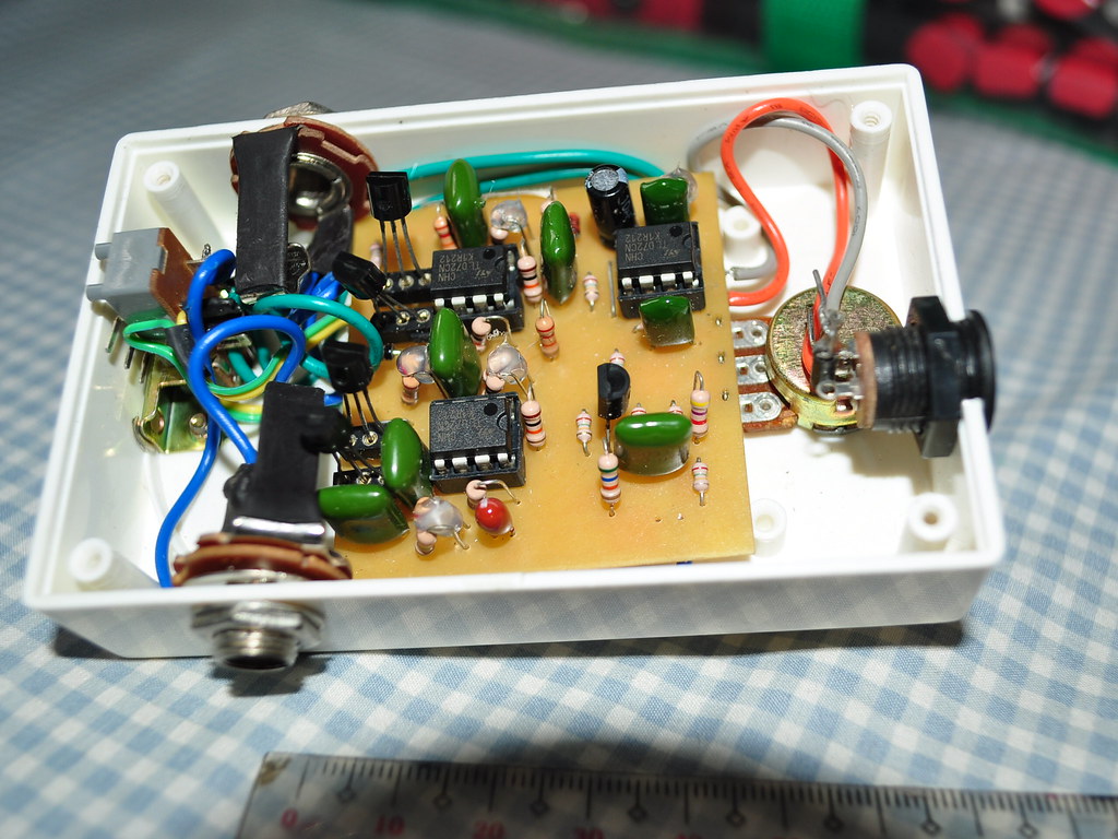
Etch your own PCB using Pre-sensintized pcb (dami pics)
hi guys,
share ko lang kung papaano ako gingawa mga pcb ko..
materials needed:
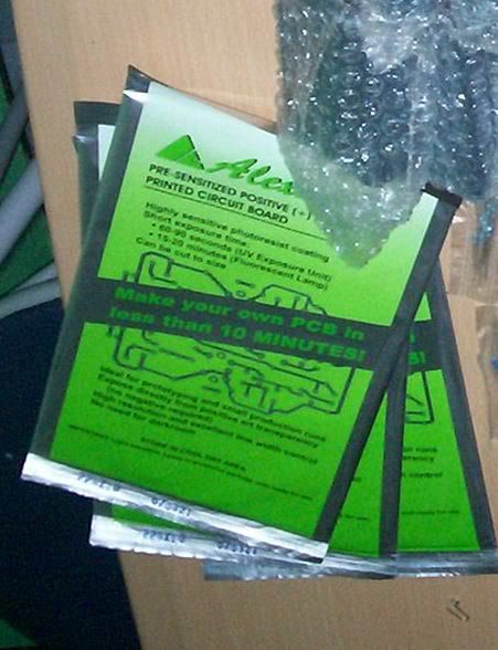
1. Pre-sensintized pcb w/ developer (from alexan)
2. Tracing Paper
3. Masking Tape
4. Bond papers
5. Clothes pins
6. Ferric Chloride (fecl)
7. Lacquer thinner
8. clear glass
sensya na po kung di masyado malinaw pagkaka-explain.. hehehe
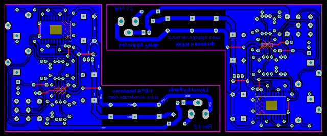
step 1: Design your pcb layout using Protel, eagle or any other software you prepare.. (i used Altium Designer 6 also know as Protel)
heto po ung HEPA Headamp na ginagawa ko.. hehe
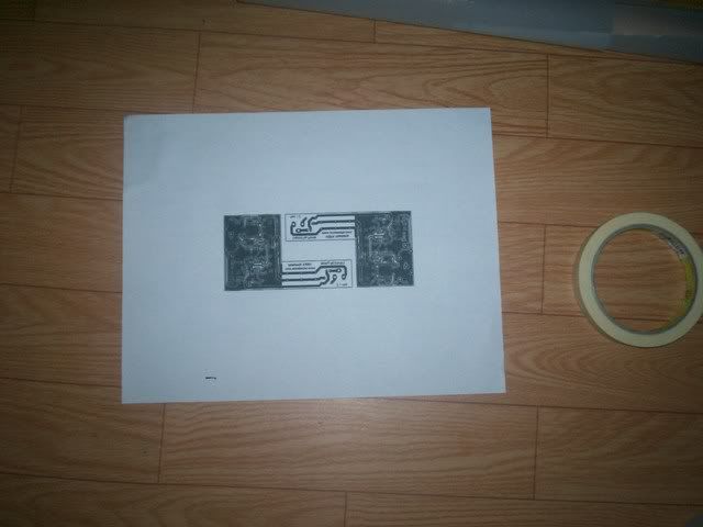
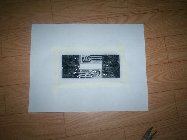
step 2: Print your layout in a piece of bond paper..
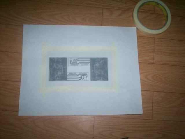
step 3: Cut a piece of tracing paper enough to cover the layout and secure it with masking tape..
step 4: Print your layout.. make sure you set your printer to maximum detail/quality
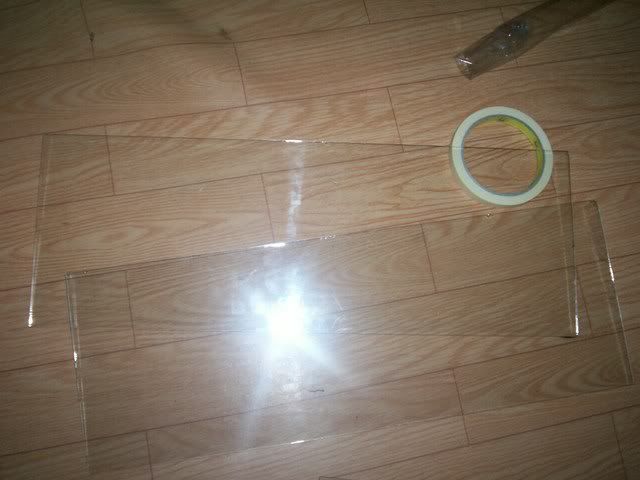
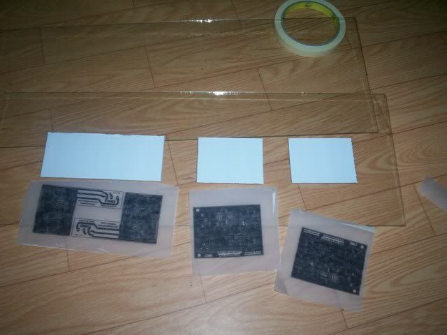
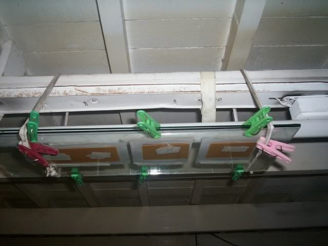
step 5: Prepare 2pcs of clear glass..
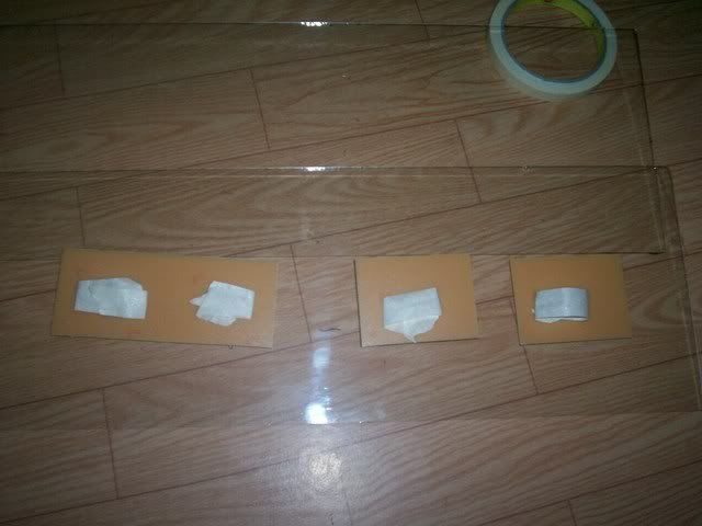
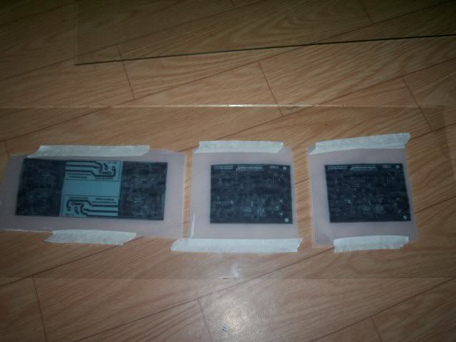
step 6: secure the pcb to the glass using masking tape..
step 7: Remove the protective film of the pcb and place the tracing paper over it..
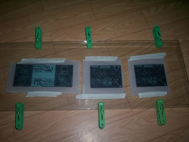
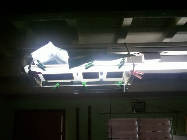
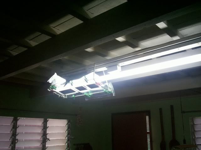
step 8: Placed the second glass over the pcb and secure with clothes pins.
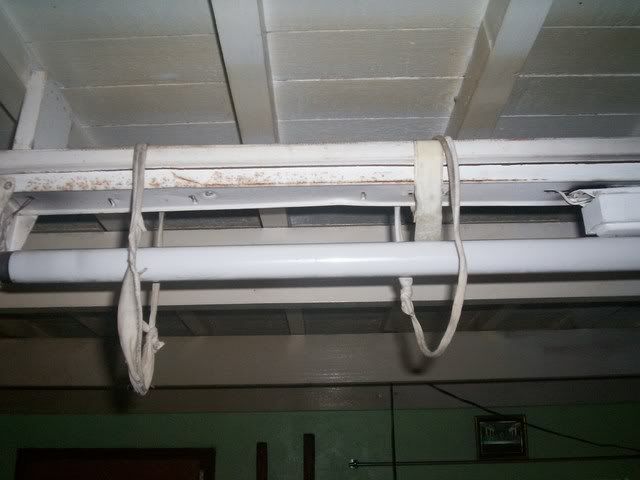
step 9: Exposed the pcb under a florescence bulb or UV exposure box for 12mins.
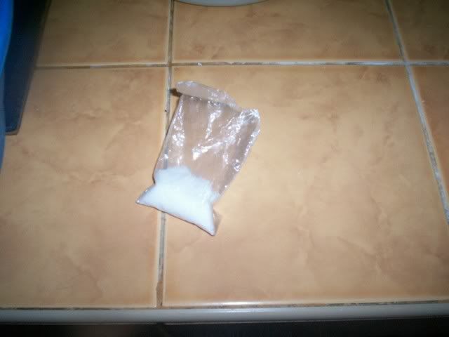
step 10: Prepare the developer solution. 1000cc 0f water per 50g of developer powder..
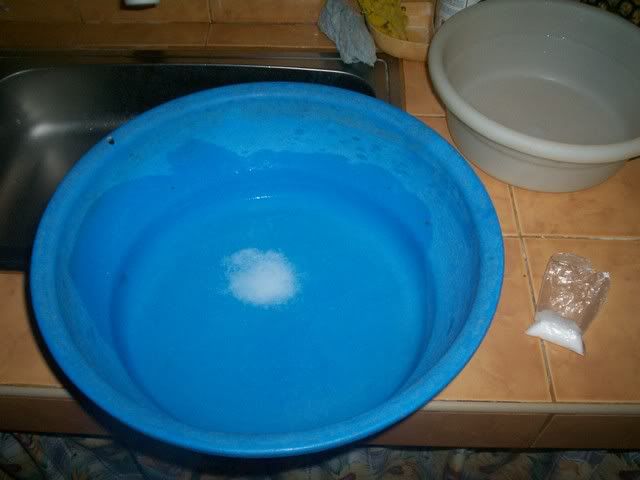
step 11: Place the pre-sensitized pcb into the solution.. Slightly shake the solution until the tracks area, clear and there is no more blue, smoke like resist coming off the exposed area on the board..
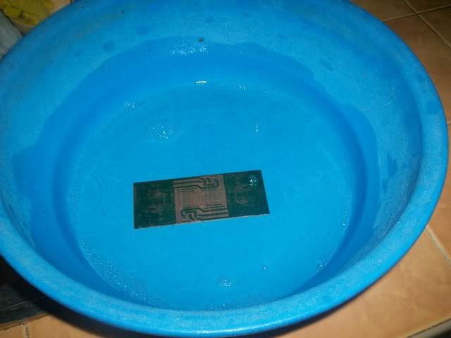
step 12: Rinse the board under running water to remove developer and to stop the developing process
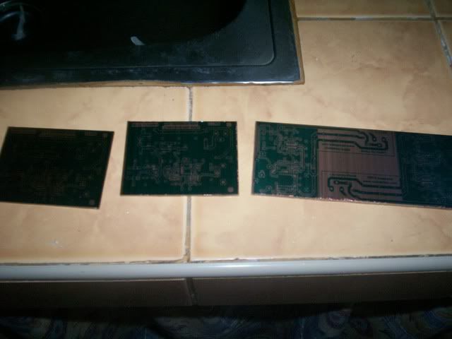
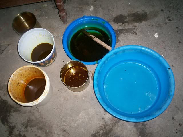
step 13: etch the PCB using ferric choloride..
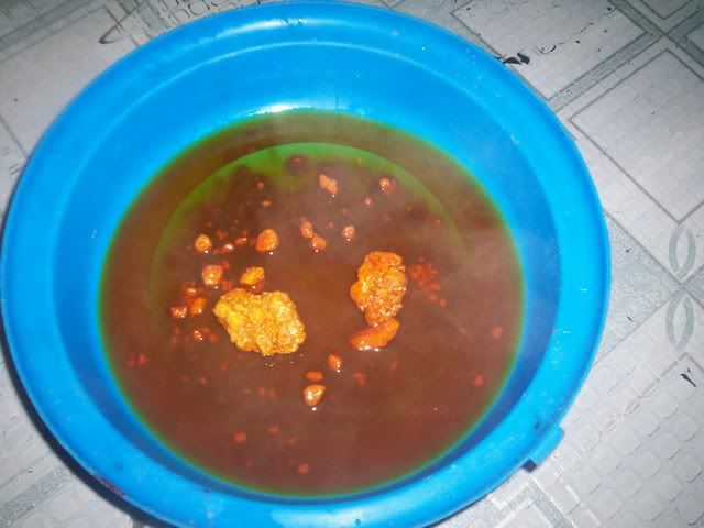
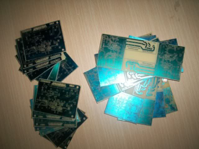
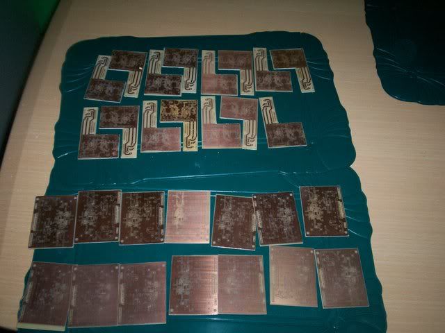
step 14: remove the photoresist coating with lacquer thinner.
sensya na po kung mali-mli grammer ko..hehehehe
share ko lang kung papaano ako gingawa mga pcb ko..
materials needed:
1. Pre-sensintized pcb w/ developer (from alexan)
2. Tracing Paper
3. Masking Tape
4. Bond papers
5. Clothes pins
6. Ferric Chloride (fecl)
7. Lacquer thinner
8. clear glass
sensya na po kung di masyado malinaw pagkaka-explain.. hehehe
step 1: Design your pcb layout using Protel, eagle or any other software you prepare.. (i used Altium Designer 6 also know as Protel)
heto po ung HEPA Headamp na ginagawa ko.. hehe
step 2: Print your layout in a piece of bond paper..
step 3: Cut a piece of tracing paper enough to cover the layout and secure it with masking tape..
step 4: Print your layout.. make sure you set your printer to maximum detail/quality
step 5: Prepare 2pcs of clear glass..
step 6: secure the pcb to the glass using masking tape..
step 7: Remove the protective film of the pcb and place the tracing paper over it..
step 8: Placed the second glass over the pcb and secure with clothes pins.
step 9: Exposed the pcb under a florescence bulb or UV exposure box for 12mins.
step 10: Prepare the developer solution. 1000cc 0f water per 50g of developer powder..
step 11: Place the pre-sensitized pcb into the solution.. Slightly shake the solution until the tracks area, clear and there is no more blue, smoke like resist coming off the exposed area on the board..
step 12: Rinse the board under running water to remove developer and to stop the developing process
step 13: etch the PCB using ferric choloride..
step 14: remove the photoresist coating with lacquer thinner.
sensya na po kung mali-mli grammer ko..hehehehe